
3D silicon chip stacks circuits vertically to boost computing power
This digest was compiled by AI from multiple sources — links to the originals are below.
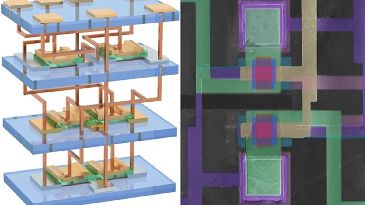
Researchers have engineered a three-dimensional silicon chip that stacks circuits in multiple layers, as detailed in a study published May 27 in Nature. The approach shortens data travel distance and reduces power consumption. It offers a path to extend Moore's law without shrinking transistors further.
Vertical Integration
The 3D chip uses ultrathin silicon membranes and low-temperature manufacturing to stack circuits directly on top of each other. This contrasts with traditional 2D chips where circuits are spread across a single surface. Lead author Qing Cao, a materials science professor at the University of Illinois Urbana-Champaign, said the method is easier and cheaper than previous stacking approaches.
Moore's Law Extension
Transistor miniaturization is hitting physical limits due to silicon's material properties and quantum mechanics, Cao noted. The contacted gate pitch — the combined width of a transistor gate and its separation from the next — is no longer shrinking. Vertical integration allows more transistors per chip without reducing individual transistor size, maintaining the trend of increasing processing power.
Heat Management
Stacking layers creates thermally dense packages, but the researchers' low-temperature fabrication technique helps mitigate overheating. The study claims the design reduces power required for data transmission between layers. Further testing is needed to assess long-term thermal stability under heavy AI workloads.
1 source
Time · lag behind first